Future Technologies
Terahertz Sensing and Communication Towards Future Intelligence Connected Networks
This paper examines the latest progress on spectrum and potential application scenarios for the THz band. A hybrid channel modeling framework for the THz band is proposed to improve modeling accuracy and efficiency.

Authors (all from Huawei 6G research team): Guangjian Wang 1, Huanhuan Gu 2, Xianjin Li 1, Ziming Yu 1, Oupeng Li 1, Qiao Liu 1, Kun Zeng 1, Jia He 1, Yan Chen 2, Jianmin Lu 1,Wen Tong 2, David Wessel 2
- Wireless Technology Lab
- Ottawa Wireless Advanced System Competency Centre
1 Introduction
The rapid development of wireless cellular communication from 1G to 5G means that it is not just people who are better connected. An increasing number of intelligent things, such as industrial equipment, cars, sensors, and home devices, are now able to connect, a trend that will continue beyond 2030, leading to the intelligent connection of everything, anywhere, all the time.
If these intelligent things also have the capability to sense their surroundings and share this information with other intelligent things, connections will become even more intelligent. Joint radar and communications technology can help achieve this, with previous research showing that co-located radar and communication systems minimize interference on each other. However, the stringent requirements on the information exchange between these two systems results in limitations in practice. Effective integrated sensing and communication (ISAC) systems, including those that are loosely coupled and those that are fully integrated, are expected to reduce system size and information exchange latency between the co-located radar and communication systems.
Each new generation uses higher spectrum with larger bandwidth, which is beneficial for sensing. If we can make THz work for 6G, many new opportunities will be possible. We believe that sensing will be one of key new services for 6G in addition to the continued expansion of 5G services.
The terahertz (THz) band (0.1–10 THz) is one of many promising pillar technologies that meets the requirements of 6G for 2030 and beyond, enabling a massive number of connected devices and providing ultra-high user data rates in the order of terabits per second (Tbit/s). This is because the THz band has ultra-large available bandwidth resources and ultra-high communication rates. Therefore, THz communication is considered to be an important alternative to air interface technology for achieving a Tbit/s communication rate. It is also expected to be applied to scenarios such as holographic communication, small-scale communication, ultra-large-capacity data backhaul, and short-distance ultra-high-speed transmission.
High-precision positioning and high-resolution sensing imaging of a network and/or a terminal device are performed by using a feature of extremely large bandwidth, which is also presents an opportunity to expand the application of THz communication.
THz can provide high-quality imaging resolution equivalent to optics (about 100 microns). THz waves can penetrate many infrared opaque materials such as paper, plastic, ceramics, and semiconductors. They can interact with molecular hydrogen bonds or van der Waals forces without any ionizing radiation, and can be used for the spectroscopic identification of organic materials. Unlike high energy X-rays, Terahertz photons are low energy (1 THz is equivalent to 4 meV) and are not harmful to people. The vibrational and rotational energy levels of molecules and the phonon vibrational energy levels of semiconductors and superconducting materials are all within the THz band, so THz waves have great advantages in spectral analysis and materials identification. Because THz can be used for both communication and sensing, it is a strong candidate for ISAC.
Compared with millimeter waves and microwaves in low frequency bands and visible light in high frequency bands, the THz channel characteristics are quite different. Compared with millimeter waves, THz waves have stronger frequency selectivity, a more obvious scattering effect, and larger transmission loss. Compared with a light wave, a THz wave has less path loss, stronger volatility, stronger reflected energy, and it is less likely to be blocked. Therefore, the existing channel models and measurement methods of millimeter waves, microwaves, and visible light systems cannot be directly applied to the THz band, which highlights the necessity of developing THz channel measurement instruments.
In the field of wireless channel modeling, there are two modeling methods:
1) Statistical channel modeling methodology based on measured data.
2) Deterministic channel modeling methodology based on ray tracing or electromagnetic (EM) field boundary solving theory.
Statistical channel modeling theory is widely used in channel modeling for mobile communication standards, such as the 3GPP standard channel model. However, the continuous development of next-generation mobile communication scenarios has increased the demand for new spectrum, which a statistical channel modeling method cannot completely meet. Therefore, deterministic channel modeling methods are being studied, with high-precision channel modeling in specific scenarios carried out using computational electromagnetics (CEM).
The device based on THz semiconductor technology mainly refers to a transistor in the THz frequency band. The solid-state circuit based on the solid-state device can implement the THz source and perform frequency mixing, frequency multiplication, and amplification on the THz signal to generate and detect the THz wave at a specific frequency.
The Schottky barrier diode (SBD) can work at normal temperature, and has a low turn-on voltage and a very short reverse recovery time. Current SBDs in the THz band are mainly based on GaAs material because of its high saturation electron rate and electron mobility. SBDs based on GaAs are used in THz solid-state active circuits. Already very mature and industrialized, they have been used by American VDI companies since the 1960s. Currently, the cutoff frequency of the component is higher than 30 THz, and the frequency mixer and frequency multiplier basically cover the THz band.
Chip integration has become the most important research direction of THz semiconductor technology. Based on semiconductor materials, semiconductor devices used in THz band amplifiers can be divided into two types: Si-based devices and III-V compound-based devices.
Si-based devices are mainly complementary metal–oxide–semiconductor (CMOS) devices and SiGe bipolar complementary metal-oxide-semiconductor (BiCMOS) devices. Group III-V compound devices include GaAs pseudomorphic high-electron-mobility transistor (PHEMT), GaAs metamorphic high-electron-mobility transistor (MHEMT), InP high-electron-mobility transistor (HEMT), InP heterojunction bipolar transistor (HBT), and GaN HEMT.
Selecting the various process and material properties for THz devices is primarily based on characteristic frequency and cutoff frequency. To select the right technology for THz applications, many parameters must be considered, including cost, output power, efficiency, the maturity of interconnection and packaging technologies, and integration capabilities. In the THz band, a large- scale antenna array is usually required to ensure transmit power. As the operating frequency increases, high integration becomes increasingly important. A small THz wavelength is highly beneficial for implementing a large-scale antenna array with a small form factor, but the small wavelength poses corresponding challenges.
To date, much progress has been made in key technological breakthroughs and prototype system development for THz communication and sensing systems. For example, Zhejiang University developed a multi-channel THz wireless communication system based on photoelectric combination. The system uses an eight-channel THz carrier for modulation to achieve ultra-high-speed wireless communications with a working frequency of 0.4 THz, a modulation method of 16QAM, and a transmission rate of 160 Gbit/s. The advantage of the system lies in achieving an ultra-high transmission rate and improving bandwidth utilization. In 2020, the University of Electronic Science and Technology of China achieved THz high-speed wireless communication with a working frequency of 0.22 THz, a communication distance of more than 1,000 m, a bit error rate of less than 1E-6, and a transmission rate of more than 20 Gbit/s. For sensing technologies, terahertz time-domain spectroscopy (THz-TDS) has been used for material characterization and process control.
This remainder of this paper is organized as follows:
- Section 2 describes the latest progress on THz spectrum and potential application scenarios.
- Section 3 covers THz channel propagation and our latest measurement and modeling results on the THz band.
- Section 4 focuses on the key components and intermediate radio frequency (IRF) architecture, including THz components and chips, THz antennas, and THz integration technologies.
- Section 5 presents the prototypes and measurement results of the THz high throughput communication and high-precision sensing system. It includes prototype description, measurement environment and configurations, and measurement results.
- Section 6 gives our conclusions and suggestions for future research.
2 THz Spectrum and Application Scenarios
THz spectrum usually refers to the frequency bands between 0.1 THz to 10 THz with a corresponding wavelength of 0.03 mm to 3 mm. It lies somewhere between microwaves and optical waves, as illustrated in Figure 1. Due to its unique position in the EM spectrum, THz has the characteristics of microwaves, including penetration and absorption, and the spectral resolution of optical waves.

Figure 1 Position of THz waves in the radio spectrum
THz spectrum has been described for some time as “the last virgin land” of radio spectrum. Only a few scientific and astronomical services are deployed in these frequency bands, especially in bands above 275 GHz. In spite of abundant spectrum and support for high transmission rates and strong anti-interference, many practical technical limitations still exist.
However, this has partially changed with the development of integrated components and circuits, and the emergence of various services that require ultra-high data rate transmission. At the World Radio Communication Conference 2019 (WRC-19), RR No. 5.564A was approved, and four globally harmonized frequency bands with a total bandwidth of 137 GHz (i.e., 275–296 GHz, 306– 313 GHz, 318–333 GHz, and 356–450 GHz) were allocated for the implementation of land mobile and fixed service application in the frequency range of 275 GHz to 450 GHz, on the basis of study outcomes of Agenda Item 1.15 (WRC- 19).
With the addition of the spectrum allocated at the previous WRCs, there are now more than 230 GHz Mobile Service spectrums. Table 1 describes the allocated mobile frequency bands with a contiguous bandwidth greater than 5 GHz.
Table 1 Allocated frequency bands of mobile service in the frequency range of 100–450 GHz
Table 1 Allocated frequency bands of mobile service in the frequency range of 100–450 GHz
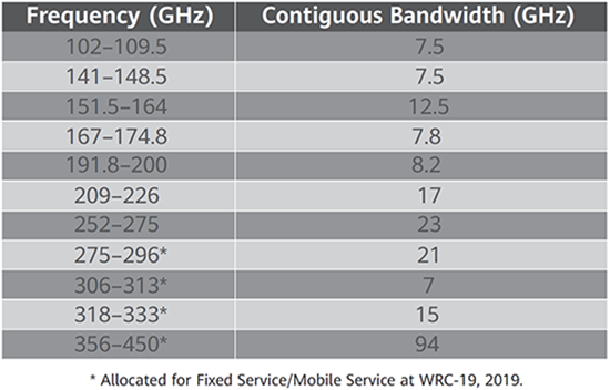
Such abundant spectrum reserves will drive the rapid development of THz communication technologies. It can facilitate extremely high-data-rate connections for existing wireless transmission applications such as fixed wireless access (FWA), wireless cellular front-haul and backhaul, and some short-range link communications. It can increase their connection rates from tens of Mbit/s or several Gbit/s to unpredictable levels that can reach hundreds of Mbit/s or even several Tbit/s, which is truly comparable to the connection capabilities of optical fiber.
Furthermore, the ultra-fine beam generated by the ultra-large-scale antenna array can be implemented in the THz frequency band, which makes high-precision positioning and high-resolution sensing possible. This will support the emergence of new services that are beyond just communication. Shorter wavelengths imply smaller antennas, so small devices can be packed with tens or hundreds of antennas, which helps estimate angles for functions like gesture recognition on smartphones. From the perspective of the base station side, enabling the sensing/imaging feature in future International Mobile Telecommunications (IMT) systems are also important application scenarios for supporting external environment recognition and map reconstruction in THz communications.
3 THz Channel Propagation and Modeling
Propagation channel modeling is a fundamental part of wireless communications. Historically, stochastic channel modeling methodology has dominated the wireless communication channel model. The stochastic channel model can describe the propagation channel using simple statistical parameters with a low computational complexity of implementation. Many projects and standards, such as 3GPP-SCM, WINNER-I/II, COST2100, and MESTIS, belong to this family. In 2015, the 3GPP 38.901 released the spatial channel model (SCM) from 0.5 GHz to 100 GHz, which became the 5G standard channel model. However, in 6G communication, the spectrum requirement has extended from millimeter-wave bands to THz bands. In THz-band channel modeling, we will face new challenges and propagation features that are quite different to those in millimeter waves.
For propagation attenuation, THz waves will experience higher path loss than millimeter waves and, in some situations, molecular absorption should be considered. In the THz band, the ultra-large bandwidth will result in frequency response inconsistency and higher delay resolution. With the frequency increase, the wavelength will decrease to the millimeter level. This implies the wavelength will be comparable with the surface roughness of most environmental furniture, so the new scattering feature should be modeled. Furthermore, new small-scale parameters, including the delay spread, angular spread, and clusters, should be restudied under the stochastic channel model.
Apart from communication, the THz band can be a candidate for sensing applications. In contrast to the communication channel, the sensing channel focuses on different parameters and methodology. For example, the imaging channel requires the deterministic channel coherence of the aperture antenna and geometry information, a feature that contradicts the traditional stochastic channel modeling approach. This means that the stochastic channel models are not suitable for sensing applications, and deterministic modeling approaches are favored. However, a single channel modeling scheme may not meet the evaluation requirements of all ISAC applications. For sensing applications, such as sensing-assisted beamforming, the stochastic modeling can be adopted. However, as the description of EM information is not required for localization and tracking cases, ray tracing is a strong candidate. On the other hand, imaging and recognition need to take the EM algorithm into account when the sizes of scatterers are approximate to wavelength.
Based on the new challenges and requirements, we propose a hybrid channel modeling methodology to support the THz band communication and sensing. Depending on different applications, different approaches are used for channel generation and system-level or link-level evaluation. A few suggested channel modeling methods are listed in Table 2.
Table 2 Terahertz channel modeling methodology

In the next section, we will introduce our current THz band channel measurement campaign progress, and relevant stochastic channel modeling results.
3.1 Channel Measurement System and Measurement Campaign
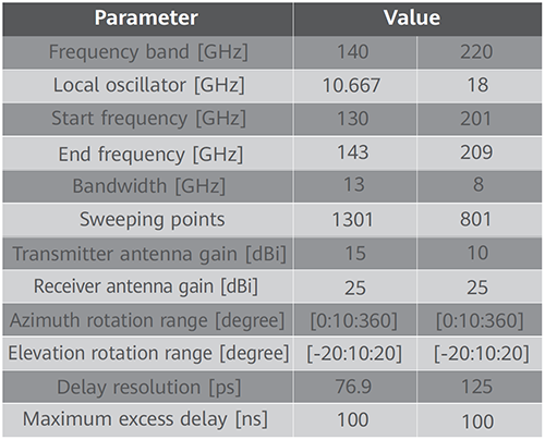
The THz channel measurement platform consists of a radio frequency (RF) front-end, with horn antennas at both the transmitter and receiver sides, and a vector network analyzer (VNA). The intermediate frequency (IF) signal is generated by the VNA and then mixed with the multiplied oscillator signal to the RF band, and finally, emitted/received by a horn antenna. With the wide bandwidth, a higher delay resolution can be achieved. To ensure wide-angle coverage, we use a wide beam width antenna at the transmitter sides. On the receiver side, a high gain antenna is mounted on a mechanical rotator to achieve the angular channel response and complement high path attenuation in the THz band. The measurement campaigns have been achieved at 140 GHz, 220 GHz, and 280 GHz. The detailed parameters are listed in Table 3.
Table 3 Parameters of the measurement system
We carry out the channel measurement in a typical meeting room and open office area. The realistic environment can be seen in Figure 2. In a meeting room with an area of 10.15 m x 7.9 m and a ceiling height of 4 m, a 4.8 m x 1.9 m table with a height of 0.77 m is placed in the center, and some chairs are placed around the table. The dimension of the office room in our channel measurement campaign is 30 m x 20 m, including a hallway and an office area. The furniture in the environment includes desks, chairs, tiny plants, and screens.

Figure 2 channel model, phased array, reconfigurable intelligent surface, THz
3.2 THz Channel Characterization and Analysis
Path loss is large-scale fading that reveals the signal power level of the receiver at different places. We evaluate the multi-frequency alpha-beta-gamma (ABG) path loss model for all the measurement sets. The multi-frequency path loss models cover the relationship between path loss and both distance and frequencies. As a widely used multi-frequency path loss model, the ABG model is obtained by adding a frequency-dependent optimization parameter to the alpha-beta (AB) model used in 3GPP. The ABG model can be expressed as
\( P L^{A B G}[d B]=10 \alpha \log _{10}\left(\frac{d}{d_{0}}\right)+\beta+10 \gamma \log _{10}\left(\frac{t}{f_{0}}\right)+X_{\sigma}^{A B G} \) (1)
Where f and \( f_{0} \) denote the carrier frequency and the reference frequency in gigahertz, respectively. d and \( d_{0} \) represent the distance between the transmitter and receiver and reference distance. \( X_{\sigma}^{A B G} \) is a zero-mean Gaussian random variable with the standard deviation \( \sigma_{S F}^{A B G} \mathrm{~dB} \), which represents the fluctuation caused by shadow fading. In addition, we can see from formula (1) that α and γ represent the dependence of path loss on distance d and frequency f, respectively, while β is an offset parameter.
Based on the measurement campaign, ABG path loss results on 140 GHz, 220 GHz, and 280 GHz bands in the meeting room environment are depicted in Figure 3. The proposed ABG path loss model is as follows:
\( P L^{A B G}[d B]=20.7 \log _{10}\left(\frac{d}{d_{0}}\right)+26.72+22.2 \log _{10}\left(\frac{f}{f_{0}}\right)+2.53 \) (2)
More measurement campaign and modeling results can be referred to in literature.
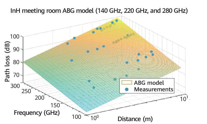
Figure 3 ABG path loss model results at the meeting room
On the small-scale aspect, the THz channel also exhibits different propagation characteristics from the millimeter wave channel. The rough surfaces at the THz band need to be considered carefully as the THz wavelength is comparable to the roughness of object surfaces. The measurements indicate that in the 140 GHz band, multipath components are still rich in the open office due to the abundance of furniture. For further study, we have chosen one receiver position (shown in Figure 4) as an example to analyze the spatial angle of arrival (AoA). We can observe that it is an obviously sparse propagation channel, in which 3 clusters are extracted with a 30-dB cutoff threshold. Furthermore, we use the ray tracing mechanism to map the clusters into the geometry space environment in Figure 4b. The propagation paths perfectly match the geometry map and measurement results. The transmitter antenna beam width is about 30°, which covers the entire area. The north direction (upwards direction on the 2D map) is defined as zero degrees with clock-wise rotation. Based on the geometry reconstruction, from the receiver point of view, the direct path is traced between the TX and RX lines with 8.7° AoA. The second path is coming from the rear left, reflected by a monitor screen, and the AoA is –160°. The third path is also a reflection path provided by the rear right monitor screen, and the AoA is 135°. There is at least 90° separation between the three paths. This implies that there are three orthogonal spatial channel streams we can utilize for beamforming design, which is good for beam management and single-user multiple-input multiple-output (SU-MIMO) performance.
Table 4 Penetration loss of different materials at 140 GHz
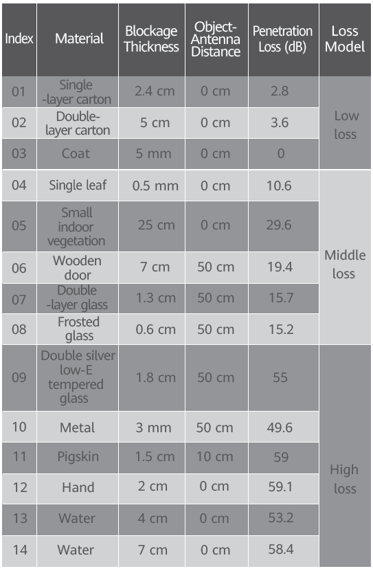

Figure 4 Indoor hotspot cell (InH) meeting room 140 GHz measurement scenario
To investigate the penetration characteristics of the THz band, we measure 14 different typical materials to study penetration loss. Three penetration loss types classified based on the analysis results are presented in Table 4. The THz wave can penetrate the carton and cotton coat easily with only several dB, even transparently. This tells us that the THz wave can be used for safety detection application, such as detecting a knife hidden in a pocket. The second category is the typical outdoor-to-indoor (O2I) material, like single-layer glass, and wooden doors. The THz wave shows above a 10-dB penetration loss which significantly affects coverage and capacity. The third category we presented is the ultra-high loss for THz waves. This kind of material contains conductive molecules that severely obstruct THz wave propagation.
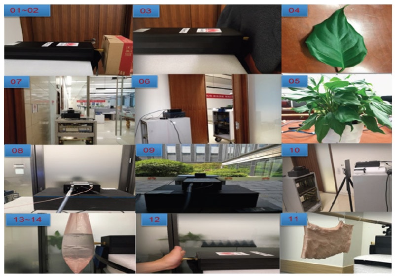
Figure 5 Penetration loss measurement for typical materials
A hybrid channel modeling methodology is proposed for THz communication and sensing. We achieve the THz-band sounding system and typical indoor measurement. The SCM-based path loss and multipath components are presented. Based on the analysis results, the THz band shows sparse spatial clustering propagation channel characteristics and sensing capabilities. In future work, we will investigate the outdoor propagation features for THz-band communication and sensing.
4 THz Hardware and Components
To meet requirements of diversified application scenarios for 6G, it is necessary to gradually industrialize THz components and key technologies, so as to realize the large-scale commercialization of the THz communication and sensing systems. The key THz components, THz antenna, intelligent surfaces, and integration technologies are investigated here.
4.1 THz Components
The "THz gap" is due to the lack of compact source and detector technology. So highly pure THz sources, high-gain and high-power amplifier that operate at the THz band and the highly sensitive THz receivers are key technologies that enable THz applications. What's exciting is that the silicon-based THz components and system have shown continued growth in sensing, imaging and communication applications beyond 100 GHz. In addition, by integrating III-V materials and devices on silicon, the system performance can further be leveraged beyond 500 GHz. Both silicon microelectronic and photonic devices can benefit from this integration approach. The different technologies available to build THz and sub-THz sources are shown in Figure 6.
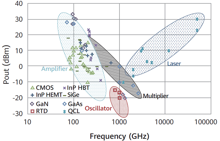
Figure 6 Terahertz gap with respect to source technology
The maximum oscillation frequency \( f_{max} \) of transistors determines the speed of the system. The demand of higher density electronics and faster system performance drives higher CMOS scaling, i.e., higher \( f_{max} \). In conventional CMOS and BiCMOS technology, the \( f_{max} \) of a transistor is between 200 GHz and 350 GHz, i.e., 45–65 nm nodes. With SiGe BiCMOS technology, the transistor can reach \( f_{max} \) of 0.5 THz, i.e., 130 nm node. Beyond \( f_{max} \), CMOS performance degrades with device scaling. Although the nonlinear effects of the device may be exploited to generate harmonic power and detect signals, efficiency is low. III-V compound semiconductors can drive \( f_{max} \) far beyond 0.5 THz. InP- based HEMTs can reach an \( f_{max} \) of 1.5 THz and double heterojunction bipolar transistors (DHBTs) can bring the \( f_{max} \) up to 1.15 THz. Another example is GaN HEMTs (\( f_{max} \) ≈ 0.58 THz).
Frequency multiplication and higher harmonic extraction from on-chip oscillators are two common ways to generate THz signals. At the THz band, planar Schottky diode technology plays a crucial role, and at room temperature, demonstrates powers of 100 μW at 1.2 THz, 15–20 μW at 1.5–1.6 THz, and 3 μW at 1.9 THz. This paper provides a comparison of state-of-the-art THz sources in CMOS and SiGe technologies, with sources for both conducted and radiated power discussed and compared. Due to the parasitic effects at the THz frequency, it is preferred that antennas are integrated on chips to simplify the packing process and prevent unnecessary signal losses. Equivalent isotropically radiated power (EIRP), defined as the product of the radiated power and directivity of the antenna radiation pattern, is used to characterize this type of THz sources. It was shown that by utilizing the power-combining technique, the radiating antenna array can significantly increase the output power, which is essential for THz beamforming and beam steering application. In a resonant tunneling diode (RTD) oscillator, the on-chip antenna is also directly decoupled for the signal-coupled output, and fundamental oscillation up to 1.98 THz and output power of 0.7 mW at 1 THz by a large-scale array have been reported.
Amplification of weak THz signals is a very important function in the system. An effective THz amplifier operates approximately 1/2 of the transistor's \( f_{max} \) and can reach 2/3 of \( f_{max} \) with proper design. Currently, amplifiers using the advanced 35 nm InP HEMT process have achieved 1.1 THz signal amplification. The power amplifiers monolithic microwave integrated circuit (MMIC) designed with the InP DHBT process can output 220 mW power at 220 GHz. Using the three-dimensional (3D) additive fabrication process, a 16-way solid state power amplifier module reaches 820 mW output at 210 GHz, making low-end THz applications possible. Figure 7 demonstrates a GaN HEMT power amplifier and its package operation at 220 GHz. The saturation output power reaches 18 dBm. Compared to the III-V counterpart, the output power and operation frequency of CMOS amplifiers are much lower. The best amplification application for CMOS is at 140 GHz, and the gain can be achieved at 200–300 GHz using positive feedback technology. BiCMOS currently operates at a maximum amplification frequency of 310 GHz, achieving 4 dBm of output power.
THz receivers can be classified as heterodyne and direct detector receivers. A heterodyne receiver down-converts the THz signal to an IF frequency driven by a local oscillator and it can acquire both phase and amplitude information from THz radiation, i.e., coherent detection. Teference paper discusses a variety of THz receivers based on both silicon and III-V technologies, ranging from 200 GHz up to near 1 THz. It showed that the InP-based receiver can generally offer similar (below 300 GHz) or better (beyond 500 GHz) performance in terms of gain and noise figure. The coherent receiver has been demonstrated in both THz imaging and communication applications.
However, practical implementation of the high-density 2D on-chip antenna array remains challenging due to system complexity and high power consumption. Moreover, multiport receiver technology is a desired feature to enable multifunction and multimode THz communication and imaging and sensing application. In the reference paper, multiport receiver technology was reviewed and different multiport architectures were discussed. A 6-port receiver system based on multiport interferometer technique was detailed, which is capable of handling AoA detection as well as data communication. This architecture can potentially find its application in future THz joint radar-communication, simultaneous localization and mapping, and imaging/sensing systems.
A direct detector can convert the illuminated THz radiation power to a measurable DC current. The receiver system usually consists of a CMOS integrated field-effect transistor (FET) or SBD with simple antennas, such as loop or patches coupled to it, and a readout circuitry that rectifies the impinging THz radiation power to a readable DC current. This paper provides comparisons of state-of-the-art direct receivers and shows that direct receivers generally have higher noise power compared to their heterodyne counterparts and are therefore mostly used in THz imaging and sensing applications. Direct receivers can better integrate with silicon in large numbers/pixels due to their simple architecture and low power consumption. They have been widely used in THz camera devices when packaged into focal-plane array configuration. The different technologies available to build THz and sub-THz receivers are shown in Figure 8.
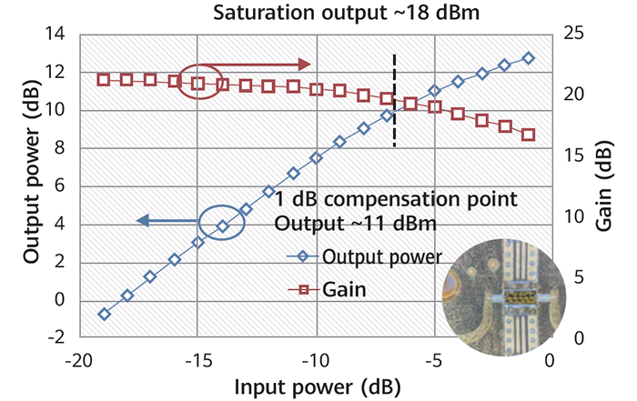
Figure 7 Output performance of 220 GHz GaN HEMT power amplifier
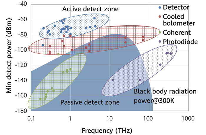
Figure 8 Terahertz receivers with respect to source technology, with 1 Hz resolution bandwidth (RBW)
4.2 THz Antenna
THz "tile-able" array is attractive as it allows for high radiated power by beam manipulations from large-scale THz antenna arrays. In a THz "tile-able" array, large number of antennas are integrated on chips to ensure the structural compactness and high power efficiency to prevent unwanted parasitic loss. In this case, the EIRP is used to indicate the effective output power of the THz source, which combines both the radiated power and directivity of array. High-level integration and scalability are two important considerations in tile design, and smartly using existing on-chip structures has become a promising approach. In the reference paper, a fully "tile-able" array was proposed that uses an existing on-chip slot mesh structure in multiple functional ways, so a high radiated power of 80 μW was achieved. Such structural multi-functionality was further leveraged in the reference paper, in which a de-centralized architecture was proposed and the scale is pushed to be comparable with that of direct detector arrays, however with an approximately 4300x sensitivity improvement. In the reference paper, a densely integrated and unified paralleled amplifier and antenna architecture was demonstrated. A patch antenna with co-existing topologically paralleled transistors was designed that can perform power radiation and amplification simultaneously. The concept was then validated using a standard 65-nm CMOS process. A set of chips were fabricated at 146 GHz and the compact unified prototypes showed an amplified radiation with 3.4-dB gain enhancement through a single element and 6-dB gain enhancement through 2×2 layout. It is also noted that frequency tuning can be achieved by varying bias.
Programmability is another desired feature of THz "tile- able" array. Limited configurability has been demonstrated mainly through electrically, mechanically, or thermally controlled reconfigurable materials. The ultimate programmability is one that can configure the transmitted THz fields digitally and receive the THz fields with arbitrary specifications. This not only includes beam synthetization with desired characteristics through beam steering or beamforming to enhance radio performance, but also includes beams with "pixelated" or "voxelated" configuration to form a desired image or video at the user end. In addition, CMOS integration is an important consideration to allow for low-cost fabrication. This reference paper proposes a THz-sensing surface with a log-periodic antenna loaded with 16 distributed detectors. By changing the detector capacitance bank configurations, the antenna is reconfigured to different working states. The system was fabricated with a standard 65-nm CMOS process and tested from a wide frequency range from 0.1–1 THz, with responsivity to different angles of direction and polarization. The reference paper demonstrates a dynamically programmable array made of split-ring resonators loaded with 8 switches fabricated using a 65 nm CMOS process. 256 states (8 bits) were reported combining both amplitude and phase control. The coded surface was shown to project simple letter holography using measured near fields. Though image resolution is low, this field projection provides a powerful approach for many applications such as sensing, qualitative imaging, and beamforming/beam steering with a silicon compatible approach.
4.3 Intelligent Surface
Signal deterioration is one of the major issues in THz communication. The high propagation loss at the THz band results in a very short communication distance. The signal blockage and misalignment impacts are more severe in the THz band. This can affect the THz network coverage and number of user accesses. Moreover, the multipath environment can cause the signal to be "null" at some locations. Therefore, an intelligent wireless system capable of adapting to a time-varying wireless environment is needed to meet these challenges.
Programmable surface is one promising candidate to provide an intelligent and controllable wireless communications system. When applied on the surface of various objects, such as buildings, it can realize various functions such as beamforming and polarization control and provide seamless connections.
In reference papers, “intelligent surface” is classified into passive surface (also termed “reconfigurable intelligent surface” (RIS)) and active surface (also termed “large intelligent surface” (LIS)). The passive RIS performs some basic functions such as beam reflection, collimation, and polarization. It operates in an energy-efficient way, since it is usually composed of low-cost passive components that are self-powered. The active LIS, on the other hand, performs the RF role partially or fully. It is usually equipped with some RF circuitry and signal processing unit which can consume power. In addition to basic beam manipulation, active LIS can further amplify the impinging wave, synthesize the desired beam pattern, and perform simple signal processing function. Intrinsically, both passive and active intelligent surfaces are made of reconfigurable radiators or scatterers. These radiators can be made of reconfigurable material, such as phase changing material or liquid crystal, or they can be controlled through a programmable interface. Either way, they enable the surface to perform in an "intelligent" way in response to wireless communication environments, which vary in time.
From the microscopic perspective, the radiator element can possess simple antenna geometry, such as loop, patch, and wire. By loading the antenna with different passive components, such as varactor diodes, through a digital controller, the working states of antenna can be changed so that their beam pattern can be steered. In reference paper, a loop antenna loaded with eight small extra loops was designed as the radiator element. Each small loop can be digitally controlled with the two states ON and OFF, and therefore 8-bit control can be realized through a programmable interface. A chip tiled with 576 such elements was fabricated, providing both amplitude and phase control, dynamic beamforming, and multi-beam formation at 0.3 THz. It was also demonstrated that the surface can project simple holographic letter images qualitatively.
Figure 9a shows a wireless communication environment enabled by intelligent surfaces. When installed on the exterior of buildings, intelligent surfaces can be used to create connections between buildings, vehicles, or automated guided vehicles (AGVs) in cases where there is no direct link between them or the link is blocked by obstacles. Intelligent surfaces can further extend radio coverage from outdoor base stations to indoor users. By programming their working states, intelligent surfaces can perform beamforming and direct beams to target end users dynamically and relay information to the desired locations with attenuation compensation. Beamforming from intelligent surfaces can also help transfer power to Internet of Things (IoT) devices and sensors.
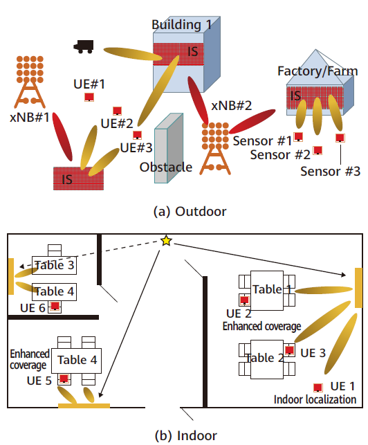
Figure 9 Typical RIS use cases for THz
When deployed in an indoor environment as shown in Figure 9b, e.g., attached to a wall, the intelligent surface can help direct the signal to the target user’s location where the signal experiences multipath fading and path loss if it is blocked by a wall or scattered by furniture, and plants. Intelligent surfaces can also be used for high-precision indoor localization as their large surface aperture can help increase location precision.
In another embodiment, the scattering elements can be of high-dielectric-index nanopillars or nanofins. Each element is modified geometrically to manipulate the amplitude, phase, and polarization of the incident EM wave. In reference paper, the working mechanism underlying this type of metasurface was discussed. The phase modulation of the transmitted wave is due to the different propagation constant of the nanopillars. For example, the induced geometric phase can occur in crossed polarized light linearly with respect to the orientation angle of the nano-element. This provides a possibility for optical holography application. The reference paper demonstrates that this all-dielectric metasurface can be used to encode the hologram by using unit element with varying orientations. Both amplitude and phase information can be recorded and controlled independently. Then, by collecting the transmitted light at the image plane, the original object can be faithfully reconstructed pixel by pixel using a standard computer-generated hologram algorithm.
Though the optical metasurface shows its ability in holography application with high fidelity image reconstruction, these surfaces are static after fabrication. A dynamic control of the holograms is desired to achieve a true holographic display. Although the concept of programmable metasurface and reconfigurable material such as phase changing material can be applied here similarly, it is still very challenging to configure pixel level wavefront representation that can reflect both phase and amplitude information of the original object dynamically in the visible spectrum. Multiplexed metasurface is another way to address this problem. There are various multiplexing methods. Wavelength division multiplexing uses nanostructures that are multiplexed in a subwavelength scale and capable of manipulating the wavefronts of multiple frequencies. Angle and polarization multiplexing can respond to light of different angles of incidence and polarization. In reference paper, an orbital angular momentum (OAM) holographic metasurface capable of reconstructing a range of OAM-dependent holographic images was demonstrated using a single meta-hologram with high spatial-resolution. It showed that incident OAM beams of 4 different modes can independently reconstruct distinctive holographic images of alphabet letters from the same multiplexed OAM meta-hologram. Recently, one reference paper demonstrated a space-multiplexed metasurface that can achieve 228 different holographic frame/image at a maximum rate of 9523 frames per second. In another reference paper, the entire metasurface is divided into many different sub-regions that are combined at different times in a specified configuration modulated by a high-speed dynamic structured laser beam modulation module to project images like an electronic meter. Strings containing digits (0 to 9) and letters can be fully reconstructed and displayed in a meaningful way using this approach.
4.4 Integration Technologies
A crucial element in the THz system is the packaging and integration technology. The most important parameters are losses and reflections in the chip-to-substrate transition. At present, the commonly used metal module package has a lower integration level and higher cost. It will be replaced by high-density integrated technologies in the future. Multichip module (MCM), system-in-package (SiP), and heterogeneous integration are promising candidates. MCMs built on high temperature co-fired ceramic (HTCC) or low temperature co-fired ceramic (LTCC) substrates have been used in THz packages. Antenna and silicon lenses are integrated in the package to reduce connection loss and enhance system EIRP. The through-silicon via (TSV) process has better integration and process precision and can be used at higher frequencies. The embedded wafer level ball grid array (eWLB) technology usually used at low frequency (with interposer or distribution layers) can also be used in the lower end of THz as SiP technology.
Silicon-based integrated circuits (ICs) prevail due to their low cost and high level of on-chip integration. III–V compound semiconductors represented by GaAs and GaN can provide a higher transmission power. A heterogeneous integration platform can provide better performance, such as higher output power, while still retaining the advantages of silicon. Wafer- level integration using Benzocyclobutene (BCB) provides a 2D integration method. The alternative approach bonds the wafer or die of III-V materials onto a patterned silicon wafer such as a 3D BCB-based wafer bonding integration scheme or wafer-scale low-temperature oxide-to-oxide bonding. These methods seem promising as they retain the advantages of silicon while leveraging the high power and high frequency operation ability of III-V semiconductor.
5 THz System and Testing
In this section, our contributions to THz communication and sensing systems are described in detail, including link simulations, testing and result analysis of THz communication, and sensing systems and prototypes.
5.1 THz Communication System
Recent technology progress in electronic, photonic and material technologies are closing the gap in THz transceiver design. Consequently, THz signal generation, modulation, and radiation methods are converging, and corresponding channel model, noise cancellation, and hardware- impairment compensation and ultra-wideband signal processing techniques for wireless communications are also emerging.
As shown in Figure 10, there are so many significant technical differences between normal frequencies and the THz band as a result of channel propagation characteristics such as large atmospheric propagation loss, strong directivity, and ultra-narrow beams. They limit signal coverage and mobile access. The impairment characteristics of broadband RF device, e.g., strong phase noise, frequency selective memory in-phase and quadrature-phase imbalance (IQI) and in-band flatness, require ingenious algorithm design. Ultra-wide bandwidth requires an ultra-high-speed analog-to-digital converter (ADC)/digital-to-analog converter (DAC) conversion rate. So, from baseband to RF, the design of a complete THz communication system is faced with great technical challenges.
It is valuable to explore novel signal processing architectures, waveform design, and corresponding compensation algorithms to solve the challenges of Ultra-High Frequency and Ultra-Wideband.
Up to now, because of the absence of experimental platforms for true THz communications, the majority of THz-band communication works are mainly theoretical and limited experimental validation. In this paper, we present our THz communication platform, i.e., the integrated testbed for ultra-broadband wireless communications at 220 GHz frequency, and the block diagram of the testbed is illustrated in Figure 11. As shown, advanced spatial and polarization multiplexing technologies are used to improve spectral efficiency.
The THz communication system consists of an RF transmitter and an RF receiver. At the transmitter, the data bits are organized in frames, modulated into symbols, undergo pre-equalization, pulse shaping, fractional delay pre-compensation, and digital IF modulation, and are fed to the high-speed DAC board. Then analog signal with a center frequency of 12.5 GHz is output. Analog IF signal is connected with the THz analog Front End.
At the receiver, the well-designed digital baseband physical algorithm is employed, the received THz signals from analog front end are digitized by the high-speed ADC boards which are synchronized, and undergo channel estimation and equalization, phase noise estimation and cancellation, interference cancellation, nonlinearity compensation, demodulation, and decoding.
A field trial experiment was conducted with a 2 × 2 polarization-MIMO in Chengdu, China. The TX/RX link distance was 330 m from the rooftop to the ground and the channel was almost line-of-sight as shown in Figure 12.
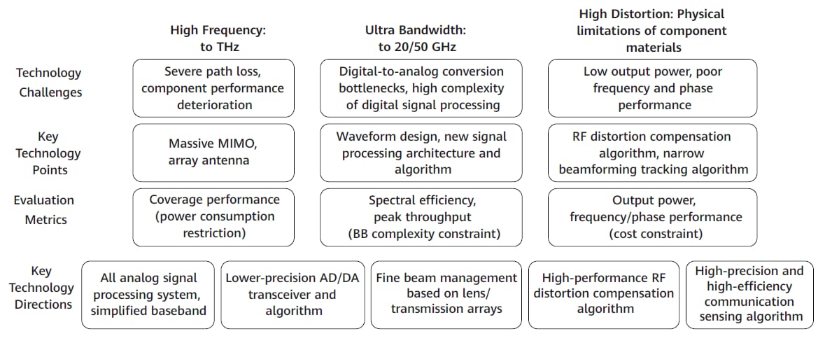
Figure 10 THz communication technical challenges
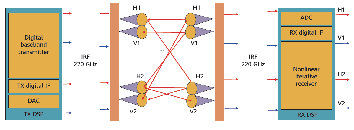
Figure 11 THz communication testbed system architecture
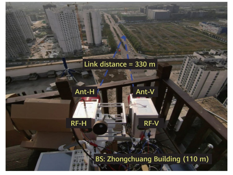
Figure 12 THz field trial, 2 × 2 polarization-MIMO system
To compensate for the constant frequency selective response of the THz RF components, a digital pre-equalization (DPEQ) filter at the transmitter is implemented. The frequency response H(k) is calculated by comparing the IF signals transmitted and received within the bandwidth of the system components:
\( H(k)=\left(\frac{P_{r}(k)-P_{n}}{P_{s}(k)}\right)^{1 / 2} \) (3)
Where \( P_{r}(k)\) is the received signal power with noise at the kth frequency, \( P_{s}(k)\) is the transmitted signal power, and \( P_{n} \) is the noise power for the whole observation bandwidth.
We theoretically and experimentally tested a time-domain DPEQ scheme for wide-bandwidth THz communication systems, which is based on the feedback of channel characteristics from the receiver-side blind and adaptive equalizers. Based on the proposed DPEQ scheme, we theoretically and experimentally studied its performance in terms of various channel conditions as well as resolutions for channel estimation. The significant improvement in channel flatness and mean squared error (MSE) performances were also demonstrated.
The channel frequency response curve is shown in Figure 13, indicating that the flatness in the signal band is irregularly fluctuating with about 16 dB maximum fluctuation in 12 GHz bandwidth. When pre-equalization is enabled, the flatness is compensated and the performance improvement noticeable.
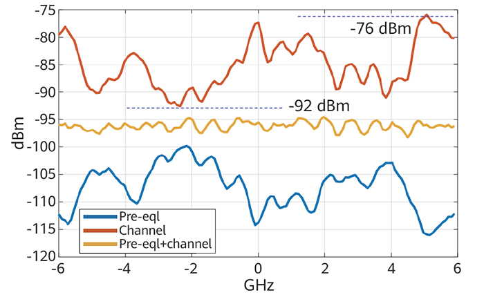
Figure 13 Channel and pre-equalization power spectral density (PSD)
The corresponding demodulation constellation is shown in Figure 14. Pre-equalization at the transmitter does not amplify channel noise, and equivalent signal-to-noise ratio (SNR) is improved. Therefore, resolution of constellation map is increased even for higher order modulation, e.g., 64QAM.
To maximize spectral efficiency and increase THz link capacity, polarization multiplexing is considered in our prototype. The vertically or horizontally polarized waves mean that the electrical field is oscillating in the vertical or horizontal direction respectively. Two ideal polarized antennas result in two independent channels, doubling the capacity of the system.
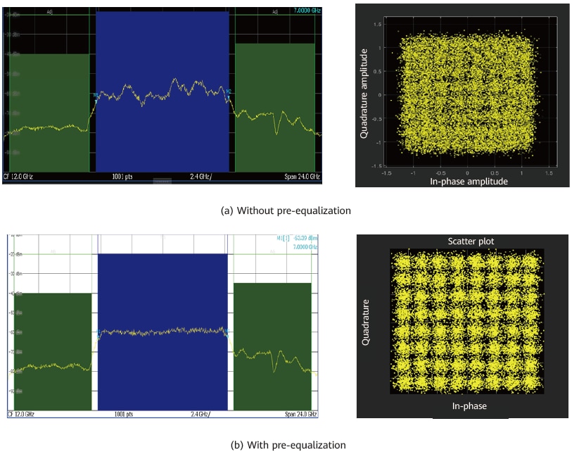
Figure 14 PSD and demodulation constellation
However, a real system always experiences imperfections such as crosstalk between polarizations. The interference between the signals inevitably occurs because of cross-polarization discrimination (XPD) of the antenna and channel degradation. This is because antenna polarization is not ideally isolated. Different polarizations may have different propagation characteristics in different channel scenarios (e.g., under raining environment), resulting in polarization leaks between channels. This leakage can be quantified using the channel XPD factor. It describes how much power from one polarization leaks into another polarization, thus reducing the system's ability to separate between the two polarizations. It is defined for the vertical and horizontal components respectively as reference paper
\( X P D_{v}=\frac{E\left\{\left|h_{v, v}\right|^{2}\right\}}{E\left\{\left|h_{H, v}\right|^{2}\right\}}, X P D_{H}=\frac{E\left\{\left|h_{H, H}\right|^{2}\right\}}{E\left\{\left|h_{v, H}\right|^{2}\right\}} \) (4)
where \( h_{V,H} \) is the flat channel impulse response between the vertically polarized transmitter and horizontally polarized receiver, with the subscripts V and H representing the vertical and horizontal antennas.
The XPD measurement is shown in Figure 15. The recording operation was performed 10 times during one day to measure the receive powers of two polarizations. The results show that mean XPD is about 19 dB with ±2 dB fluctuation influenced by mechanical deformation and beam misalignment.
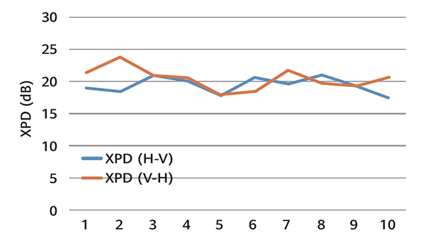
Figure 15 XPD measurement
To eliminate this interference, cross-polarization interference cancellation (XPIC) technology is used to receive signals horizontally and vertically. The signals in the two directions are then processed and the original signals recovered from the interfered signals. The assignment of the same frequency to both the vertical and horizontal polarization on a link is allowed.
The consistency of RF components is difficult to achieve since signal bandwidth is very wide, in-band channel characteristics differences between H polarization and V polarization are large, and impairment between the effect of XPD and the frequency selectivity of the channel is coupled. It is necessary to design an ultra-large bandwidth polarization interference cancellation algorithm.
Polarization interference cancellation performance is shown in Figure 16. It can be observed that the contrast convergence curve in time domain is stable and it has a performance gain of about 2 dB.
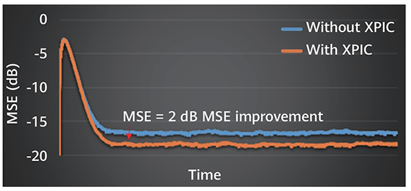
Figure 16 Polarization interference cancellation performance
Classical coherent architectures are combined with high spectral efficiency schemes. This entails numerous constraints on the design of RF components especially at the oscillator level. Indeed, high frequency oscillators severely impair THz systems with phase noise.
There are several different methods to model the random process of phase noise such as the well-known Wiener random process and Gaussian random process. In our design, to model the influence of phase noise, a zero-mean White Gaussian Noise is first generated and then passed through an infinite impulse response (IIR) filter. After that, the filtered noise is added to the angle component of the input signal. This generation process is shown in Figure 17, in which \(F_{0} \) is the frequency offset, phase_noise is the prescribed phase noise level at the frequency offset \(F_{0} \), \(F_{s} \) is the sampling frequency, and K is the gain factor controlling the phase noise level at the frequency offset \(F_{0} \).
\( \phi(n)=\phi(n-1)+K_{w}(n) \) (5)
The power spectrum of the phase noise \( e^{j \phi(n)} \) is equal to
\( \mathrm{P}(f)=\frac{1}{F_{s}} \cdot \frac{1-e^{-K^{2}}}{1+e^{-K^{2}}-2 e^{-k^{2} / 2} \cos \left(2 \pi \frac{f}{F_{s}}\right)} \cdot \operatorname{rect}\left(\frac{f}{F_{s}}\right) \) (6)
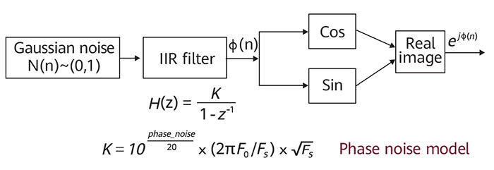
Figure 17 Phase noise model
Normally, in a multi-channel system, the phase noise in each channel will be independent of each other due to the distributed local oscillator in each channel. It will degrade system performance, and new phase estimation and compensation schemes will be invoked to solve this problem. A specially constructed pilot code is used to project the mixed phase noise onto the space-time orthogonal code space. The distributed Master and Slave phase-locked loop (MS-PLL) and quasi-linear interpolation phase noise suppression (PNS) algorithms are used to track and compensate the phase noise in the multi-channel signal space dimension, which is a low overhead (< 5% pilot proportion) solution that is able to suppress typical distributed independent phase noise.
Although THz frequency oscillators have an absolute strong phase noise, a higher symbol rate means a shorter symbol switching time, and a stronger phase noise correlation between consecutive symbols.
As shown in Figure 18, the powerful MS-PLL architecture can greatly track and compensate for the impact of phase noise. When MS-PLL is enabled, the pilot interval is changed and the impact is not obvious. Compare pilot interval 16 with 256, the performance gap is not more than 1 dB.
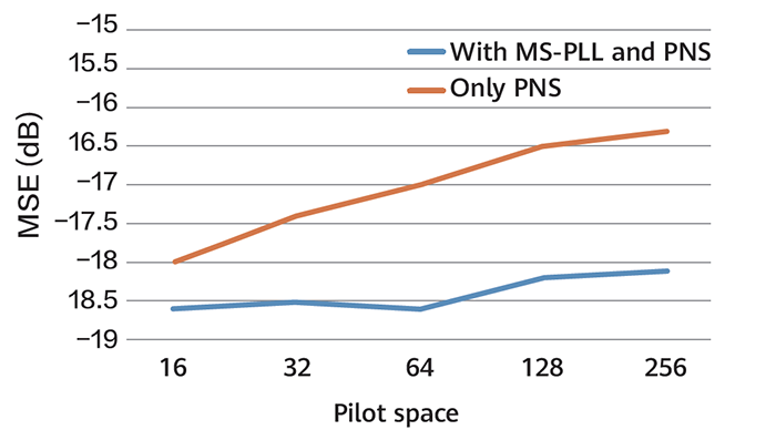
Figure 18 PNS performance
Due to the narrow beam (3 dB beam-width is only 1o), mechanical installation and antennas alignment are particularly important to support sufficient receive power. In Figure 19, the transmit power is 16 dBm and the antenna gain is 43 dBi. According to the link budget, for a 330 m link distance, the RX antenna ports should receive power of –43.6 dBm. Considering the line loss and atmospheric absorption, the measured receive power is –46.7 dBm.
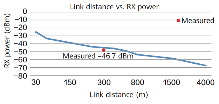
Figure 19 Receive power vs. Link distance
For medium distance outdoor transmission experiments over a distance of 330 m, we connected small 43 dBi lens antennas to the THz-wireless front-ends. At the receiver, the modem implements digital signal processing (DSP) to mitigate the effects of transmission impairments, considering both single-carrier and orthogonal frequency- division multiplexing (OFDM). The measurement results show a different Baud rate from 4 GBd to 17.5 GBd. The reference curves correspond to a bit error rate (BER) at the experimentally used soft-decision forward error correction (SD-FEC) threshold of 2.1E-2, which can be achieved assuming error-free decoding with a 20% overhead. From the performance comparison results, single-carrier is superior to OFDM since the former has a small peak-to-average ratio and is less sensitive to phase noise.
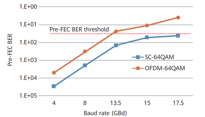
Figure 20 Pre-BER performance
Maximum throughput is 210 Gbit/s (17.5 x 4 x 2) and net data rate is 168 Gbit/s (210 x (1 – 0.2)). After removal of the forward error correction (FEC) overhead, the corresponding demodulated constellation is shown in Figure 21.
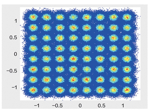
Figure 21 64QAM demodulated constellation
In addition, due to sufficient transmit power, high-gain antenna, and high-sensitivity DSP algorithm, our verification also includes the long-distance field trial for single-input single-output (SISO). As shown in Figure 22, the link distance is 3.6 km with humid weather conditions.
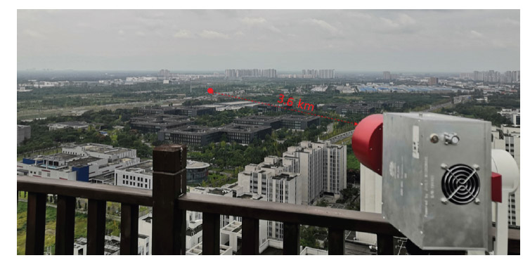
Figure 22 3.6 km long distance test
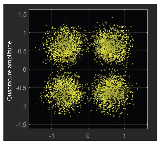
Figure 23 3.6 km, demodulation constellation
The corresponding link budget can be found in Table 5.
Table 5 Corresponding link budget
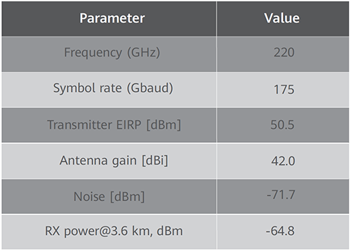
Maximum throughput is 35 Gbit/s and net data rate is 28 Gbit/s after the FEC overhead is removed.
To explore the goal of realizing the ISAC in THz, we use a similar system architecture and device to carry out sensing experiment. By using the concept of virtual MIMO and compression-sensing algorithms, the EM imaging of metal objects hidden in a paper box is rebuilt successfully, and mm-level imaging resolution is achieved.
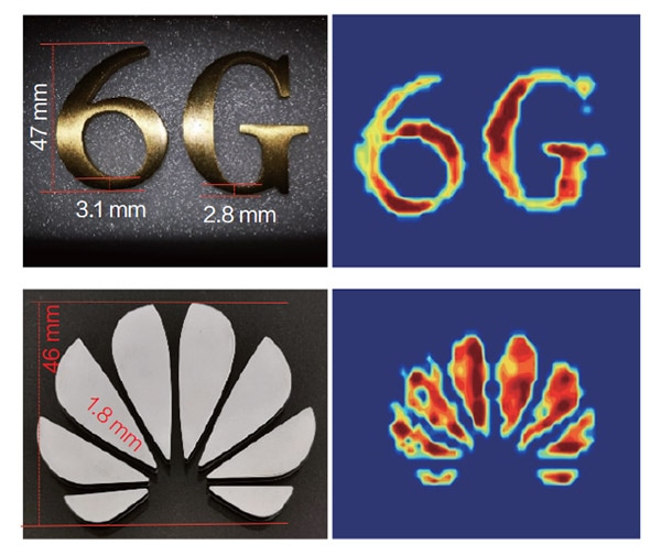
Figure 24 channel model, phased array, reconfigurable intelligent surface, THz
5.2 THz Sensing System
Material characterization is a potential THz application that can be used to study properties of dielectric materials. The THz-TDS allows non-invasive measurement of various material parameters through mathematical operations, sending a broadband pulse signal to the material sample and measuring the output signal either in transmission or reflection mode. We developed both the simulation model and measurement setup for the THz-TDS material characterization application.
CST Microwave Studio was used as simulation tool for THz-TDS setup. In the EM model as shown in Figure 25, two lens bow-tie antennas were designed and placed at each side of a dielectric Polytetrafluoroethylene (PTFE) sample. Then a time-domain simulator was set up and both simulations with and without the sample were performed. After the simulation, both reference signal (without the sample) and output signal (with the sample) and the input pulse were collected and sent to an optimization algorithm to solve for the material properties, i.e., permittivity and loss tangent. Here, the Nelder-Mead algorithm was applied at each frequency to solve the material property. It is shown that both the permittivity and loss tangent extracted from the signal agree with the theoretical values.
The reference paper demonstrates a quasi-optical system that performs complex material property measurement at sub-THz. As shown in Figure 25, a set of two-parabolic-mirror system and four parabolic-mirror system was developed. Two 80 mm-length corrugated horn antennas were designed to achieve a wide plane wave zone. After obtaining the S parameters at both ports, a closed mathematical form expression based on multiple reflection models was applied to calculate the complex material property. The complex permittivity of various Rogers RT/duroid series printed circuit board (PCB) substrates agree with the literature.

Figure 25 Simulated and measurement results of material characterization application; measurement from reference paper
THz imaging is promising for biomedical applications due to the non-ionizing THz radiation. Fast and efficient image reconstruction algorithms can help accelerate the imaging acquisition speed. In this paper, a qualitative microwave holography (QMH) imaging method was demonstrated to perform the imaging and material mapping application. QMH is a real-time direct inversion algorithm that can reconstruct the object image from all the S parameter measurements on the image plane. The S parameters are then used in two linearization models, Born's and Rytov's approximations, to reconstruct the object image and map its complex material property.
The following image test-bed was then set up to validate the QMH method, as shown in Figure 26. Nylon and metal balls were set up, with diameters ranging from 1 mm to 3 mm and the separation distance ranging from 5 mm to 20 mm. Four S parameters were collected in 2-port measurements with a frequency sweep from 26 GHz to 40 GHz. It is shown that QMH can achieve spatial resolution close to λ/4, even under a far-field measurement setup. A comparison of Born and Rytov approximation in image qualities can be found in reference papers.
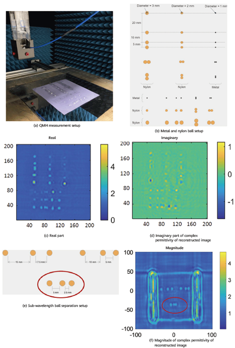
Figure 26 QMH reconstruction of metal and nylon balls of various sizes. Results from the reference paper
6 Conclusion
In this paper, we discussed the advantages and typical scenarios of THz communication and sensing application. We also proposed a hybrid channel modeling framework to improve the modeling accuracy and efficiency at the THz frequency. In particular, the THz subsystem with silicon and III-V compound semiconductor materials heterogeneous integration is analyzed and we propose to improve performance by using the advantages of different processes and materials. Finally, the prototype and measurement campaigns were conducted to illustrate the advantages of THz frequency for high-throughput communication and high-resolution sensing scenarios. A variety of measurement campaign examples show a 210-Gbit/s data transmission rate at a distance of 330 m and up to 3 mm invisible imaging, which achieves the highest performance in this field.
Future work will concentrate on following topics:
- Unified channel modeling frameworks and parameters compatible for all frequency bands and all application scenarios
- Unified air-interface and signal processing frameworks
- Technologies to improve the operating frequency and output power of components and low-cost large array solutions at the THz frequency
- Real-time prototypes and field trial with multiple points to further study the performance advantages of THz frequency for 6G in the future.
- Tags:
- 6G


